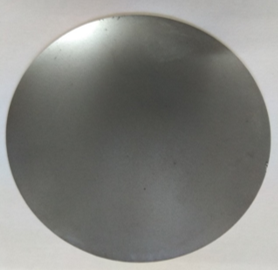
METHOD FOR HIGH-TEMPERATURE BONDING OF SILICON WAFERS FOR FORMATION KNI STRUCTURE IN MICROELECTRONICS
 Description: Laboratory technology for high-temperature bonding (1200 °C) of single-crystal silicon wafers has been developed.
Bonding is performed using a composition based on silicon dioxide, which is applied to the connected surfaces by spraying.The glass-forming composition was prepared using sol-gel technology, which reduces the glass-forming temperature.
Technical characteristics of the glass for bonding silicon wafers:
- thickness– 100-200 μm;
- density– 2,10 g/cm3;
- relative permittivity (28 Hz, 39 Hz) –3,52 ± 0,1.
Advantage: The use of glass reduces the requirements for the quality of processing and washing of joined surfaces, makes it possible to connect different surfaces and simplify the process of preparation and bonding.
Advantages of this process: simplicity and compatibility with Al metallization.
This technology makes it possible to obtain SOI structures (silicon on an insulator) for the production of integrated circuits with increased radiation and thermal stability, various sensors and elements of microelectromechanical systems for special applications.
Readiness degree:
Experimental samples obtained.
VLADIMIR GAISHUN
HEAD OF ADVANCED MATERIALS RESEARCH LABORATORY
CANDIDAT OF PHYSICS AND MATHEMATICS, DOCENT
TEL. +(375 232) 50-38-22, FAX +(375 232) 50-38-13,
E-MAIL: VGAISHUN@GSU.BY, http://pnil.gsu.by/
QR code for this page:
